Microcones on silicon, SEM
Bildnummer 14115206
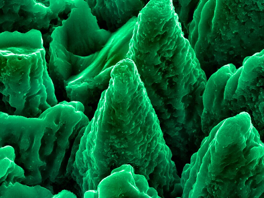
| Microcones on silicon. Coloured scanning electron micrograph (SEM) of microcones formed on a silicon surface by a laser beam. This research involves the use of lasers to etch and ablate metal and semiconductor surfaces. The resulting microstructures and nanostructures can have applications in various forms of electronics and nanotechnology. | |
| Lizenzart: | Lizenzfrei |
| Credit: | Science Photo Library / GEORGY SHAFEEV |
| Modell-Rechte: | nicht erforderlich |
| Eigentums-Rechte: | nicht erforderlich |
| Restrictions: | - |
Preise für dieses Bild ab 29 €
Für digitale Nutzung (72 dpi)
ab 29 €
Für Druckauflösung (300 dpi)
ab 300 €