Nanoparticle layer microelectronics
Bildnummer 12992028
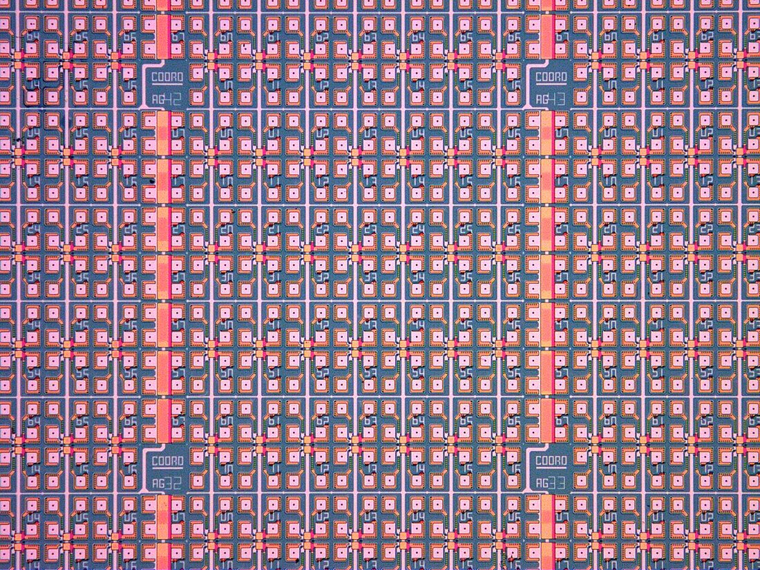
| Nanoparticle layer microelectronics. Array of metallic nanoparticle contacts developed to allow molecular monolayer electronic devices. This method allows molecular integration on conventional silicon chips, using the standard fabrication methods of the semiconductor industry. Image published in July 2018. | |
| Lizenzart: | Lizenzpflichtig |
| Credit: | Science Photo Library / IBM Research |
| Bildgröße: | 3748 px × 2811 px |
| Modell-Rechte: | nicht erforderlich |
| Eigentums-Rechte: | nicht erforderlich |
| Restrictions: | - |
Preise für dieses Bild ab 15 €
Universitäten & Organisationen
(Informationsmaterial Digital, Informationsmaterial Print, Lehrmaterial Digital etc.)
ab 15 €
Redaktionell
(Bücher, Bücher: Sach- und Fachliteratur, Digitale Medien (redaktionell) etc.)
ab 30 €
Werbung
(Anzeigen, Aussenwerbung, Digitale Medien, Fernsehwerbung, Karten, Werbemittel, Zeitschriften etc.)
ab 55 €
Handelsprodukte
(bedruckte Textilie, Kalender, Postkarte, Grußkarte, Verpackung etc.)
ab 75 €
Pauschalpreise
Rechtepakete für die unbeschränkte Bildnutzung in Print oder Online
ab 495 €