Nanostructures on metal, SEM
Bildnummer 12394549
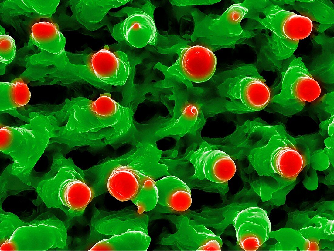
| Nanostructures on metal. Coloured scanning electron micrograph (SEM) of nanostructures formed on a metal surface by a laser beam. This research involves the use of lasers to etch and ablate metal and semiconductor surfaces. The resulting nanostructures can have applications in various forms of electronics and nanotechnology. | |
| Lizenzart: | Lizenzpflichtig |
| Credit: | Science Photo Library / GEORGY SHAFEEV |
| Bildgröße: | 6809 px × 5133 px |
| Modell-Rechte: | nicht erforderlich |
| Eigentums-Rechte: | nicht erforderlich |
| Restrictions: | - |
Preise für dieses Bild ab 15 €
Universitäten & Organisationen
(Informationsmaterial Digital, Informationsmaterial Print, Lehrmaterial Digital etc.)
ab 15 €
Redaktionell
(Bücher, Bücher: Sach- und Fachliteratur, Digitale Medien (redaktionell) etc.)
ab 30 €
Werbung
(Anzeigen, Aussenwerbung, Digitale Medien, Fernsehwerbung, Karten, Werbemittel, Zeitschriften etc.)
ab 55 €
Handelsprodukte
(bedruckte Textilie, Kalender, Postkarte, Grußkarte, Verpackung etc.)
ab 75 €
Pauschalpreise
Rechtepakete für die unbeschränkte Bildnutzung in Print oder Online
ab 495 €