Metal crater formed by a laser, SEM
Bildnummer 12394538
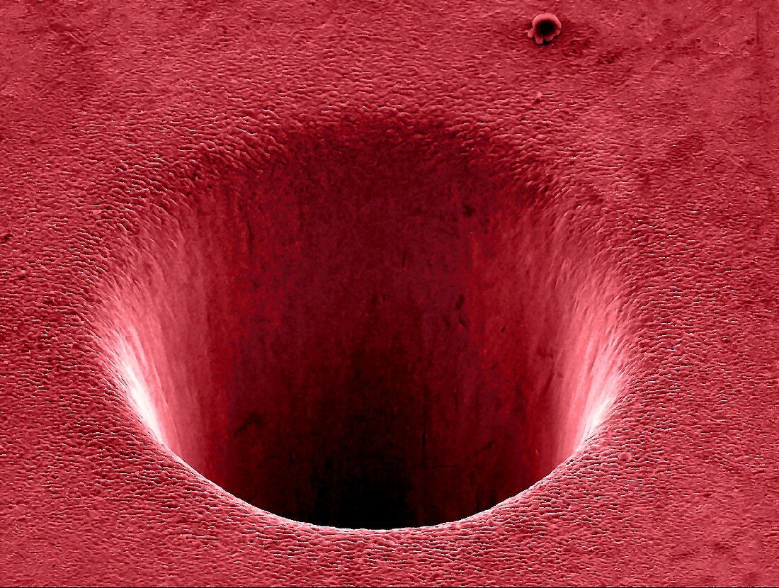
| Metal crater formed by a laser. Coloured scanning electron micrograph (SEM) of a nanoscale crater formed on a metal surface by a picosecod laser beam. This crater was produced during research that involves the use of lasers to etch and ablate metal and semiconductor surfaces. The resulting nanostructures can have applications in various forms of electronics and nanotechnology. | |
| Lizenzart: | Lizenzpflichtig |
| Credit: | Science Photo Library / GEORGY SHAFEEV |
| Bildgröße: | 6805 px × 5136 px |
| Modell-Rechte: | nicht erforderlich |
| Eigentums-Rechte: | nicht erforderlich |
| Restrictions: | - |
Preise für dieses Bild ab 15 €
Universitäten & Organisationen
(Informationsmaterial Digital, Informationsmaterial Print, Lehrmaterial Digital etc.)
ab 15 €
Redaktionell
(Bücher, Bücher: Sach- und Fachliteratur, Digitale Medien (redaktionell) etc.)
ab 30 €
Werbung
(Anzeigen, Aussenwerbung, Digitale Medien, Fernsehwerbung, Karten, Werbemittel, Zeitschriften etc.)
ab 55 €
Handelsprodukte
(bedruckte Textilie, Kalender, Postkarte, Grußkarte, Verpackung etc.)
ab 75 €
Pauschalpreise
Rechtepakete für die unbeschränkte Bildnutzung in Print oder Online
ab 495 €