Semiconductor manufacture
Bildnummer 11894766
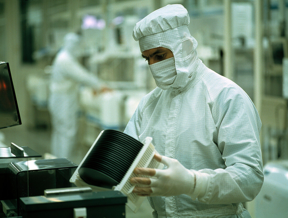
| Semiconductor manufacture. Technician in a clean room facility inspecting silicon wafers for use in semiconductor devices in the electronics industry. The wafers must be made from high-quality crystals of precisely controlled orientation and electrical properties. Photographed in Germany | |
| Lizenzart: | Lizenzpflichtig |
| Credit: | Science Photo Library / Maximilian Stock |
| Bildgröße: | 4311 px × 3267 px |
| Modell-Rechte: | Derzeit liegt noch kein Release vor. Bitte kontaktieren Sie uns vor Verwendung. |
| Eigentums-Rechte: | nicht erforderlich |
| Restrictions: |
|
Preise für dieses Bild ab 15 €
Universitäten & Organisationen
(Informationsmaterial Digital, Informationsmaterial Print, Lehrmaterial Digital etc.)
ab 15 €
Redaktionell
(Bücher, Bücher: Sach- und Fachliteratur, Digitale Medien (redaktionell) etc.)
ab 30 €
Werbung
(Anzeigen, Aussenwerbung, Digitale Medien, Fernsehwerbung, Karten, Werbemittel, Zeitschriften etc.)
ab 55 €
Handelsprodukte
(bedruckte Textilie, Kalender, Postkarte, Grußkarte, Verpackung etc.)
ab 75 €
Pauschalpreise
Rechtepakete für die unbeschränkte Bildnutzung in Print oder Online
ab 495 €