Quality control of integrated circuit wafers
Bildnummer 11894732
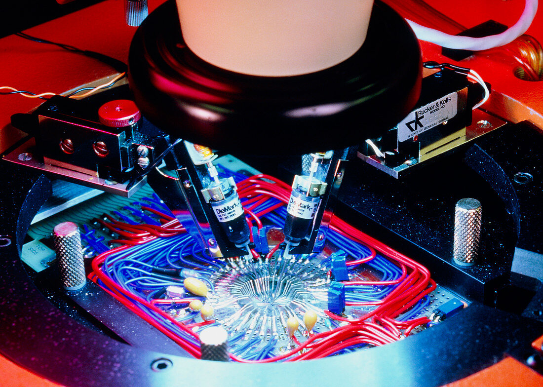
| Quality control stage in the fabrication of silicon-based integrated circuit wafers,showing a close-up of a probe which automatically test the circuitry of each chip on the wafer. Any chips that are found to be faulty are marked with ink contained in the two pens visible in centre. After probing,a wafer is baked to harden the ink; defective chips may then be identified and discarded when the wafer is sawn into individual integrated circuits,ready for the attachment of connector wires and final packaging (encapsulation) | |
| Lizenzart: | Lizenzpflichtig |
| Credit: | Science Photo Library / SEAGATE MICROELECTRONICS LTD / DAVID PARKER |
| Bildgröße: | 3543 px × 2526 px |
| Modell-Rechte: | nicht erforderlich |
| Eigentums-Rechte: | nicht erforderlich |
| Restrictions: | - |
Preise für dieses Bild ab 15 €
Universitäten & Organisationen
(Informationsmaterial Digital, Informationsmaterial Print, Lehrmaterial Digital etc.)
ab 15 €
Redaktionell
(Bücher, Bücher: Sach- und Fachliteratur, Digitale Medien (redaktionell) etc.)
ab 30 €
Werbung
(Anzeigen, Aussenwerbung, Digitale Medien, Fernsehwerbung, Karten, Werbemittel, Zeitschriften etc.)
ab 55 €
Handelsprodukte
(bedruckte Textilie, Kalender, Postkarte, Grußkarte, Verpackung etc.)
ab 75 €
Pauschalpreise
Rechtepakete für die unbeschränkte Bildnutzung in Print oder Online
ab 495 €