Scientist inspecting special coating system
Bildnummer 11894724
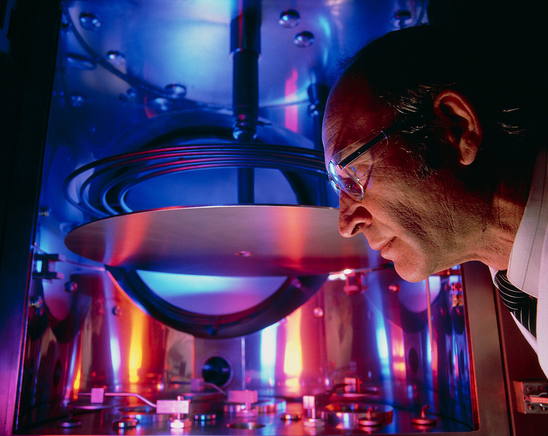
| Scientist inspecting a component of a special coating system under development in the laboratory at Edwards High Vacuum (a member of The BOC Group) Crawley,U.K. High vacuum technology is a requirement of the semiconductor industry. Vacuum chambers are used to deposit thin metallic films onto silicon wafers during the manufacture of individual integrated circuits (silicon chips). Circular silicon wafers,typically 2-3 inches in diamter are used as the building-blocks of the "chips",which are diced from the completed wafers | |
| Lizenzart: | Lizenzpflichtig |
| Credit: | Science Photo Library / Fielding, Malcolm / The Boc Group |
| Bildgröße: | 4724 px × 3759 px |
| Modell-Rechte: | Derzeit liegt noch kein Release vor. Bitte kontaktieren Sie uns vor Verwendung. |
| Eigentums-Rechte: | nicht erforderlich |
| Restrictions: | - |
Preise für dieses Bild ab 15 €
Universitäten & Organisationen
(Informationsmaterial Digital, Informationsmaterial Print, Lehrmaterial Digital etc.)
ab 15 €
Redaktionell
(Bücher, Bücher: Sach- und Fachliteratur, Digitale Medien (redaktionell) etc.)
ab 30 €
Werbung
(Anzeigen, Aussenwerbung, Digitale Medien, Fernsehwerbung, Karten, Werbemittel, Zeitschriften etc.)
ab 55 €
Handelsprodukte
(bedruckte Textilie, Kalender, Postkarte, Grußkarte, Verpackung etc.)
ab 75 €
Pauschalpreise
Rechtepakete für die unbeschränkte Bildnutzung in Print oder Online
ab 495 €