Wafer of single-crystal silicon
Bildnummer 11894522
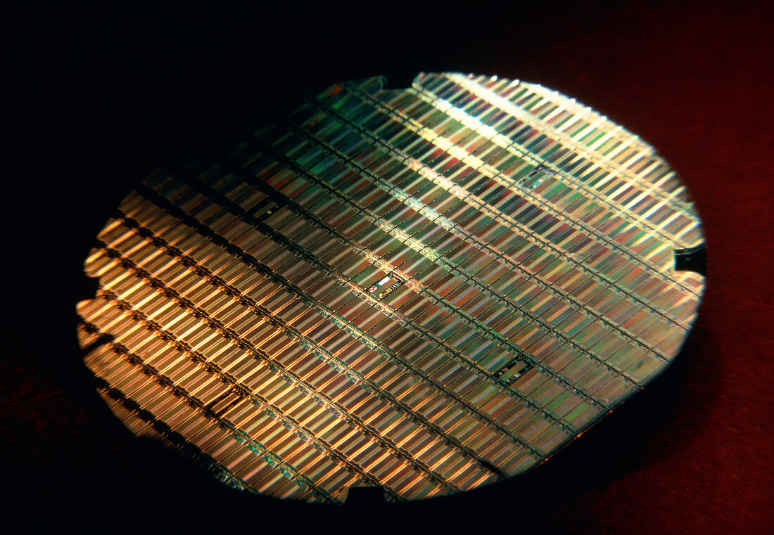
| Wafer of single-crystal silicon on which there are approximately 300 usable 16K memory integrated circuits (silicon chips). The 5 small rectangles which appear different are the process control modules - test areas for monitoring the wafer's progress through its many manufacturing stages. The 4 vacant areas positioned around the edge of the 7.6 cm diameter wafer are for handling. The flat edge (bottom right) marks the crystallographic axis of the silicon,which is important in the layout of the wafer. When completed,the wafer is inscribed with a diamond in the narrow lanes between the chips & then "diced" into single chips for packaging | |
| Lizenzart: | Lizenzpflichtig |
| Credit: | Science Photo Library / Walsh, John |
| Bildgröße: | 3453 px × 2390 px |
| Modell-Rechte: | nicht erforderlich |
| Eigentums-Rechte: | nicht erforderlich |
| Restrictions: | - |
Preise für dieses Bild ab 15 €
Universitäten & Organisationen
(Informationsmaterial Digital, Informationsmaterial Print, Lehrmaterial Digital etc.)
ab 15 €
Redaktionell
(Bücher, Bücher: Sach- und Fachliteratur, Digitale Medien (redaktionell) etc.)
ab 30 €
Werbung
(Anzeigen, Aussenwerbung, Digitale Medien, Fernsehwerbung, Karten, Werbemittel, Zeitschriften etc.)
ab 55 €
Handelsprodukte
(bedruckte Textilie, Kalender, Postkarte, Grußkarte, Verpackung etc.)
ab 75 €
Pauschalpreise
Rechtepakete für die unbeschränkte Bildnutzung in Print oder Online
ab 495 €