Scanning electron microscope
Bildnummer 11832531
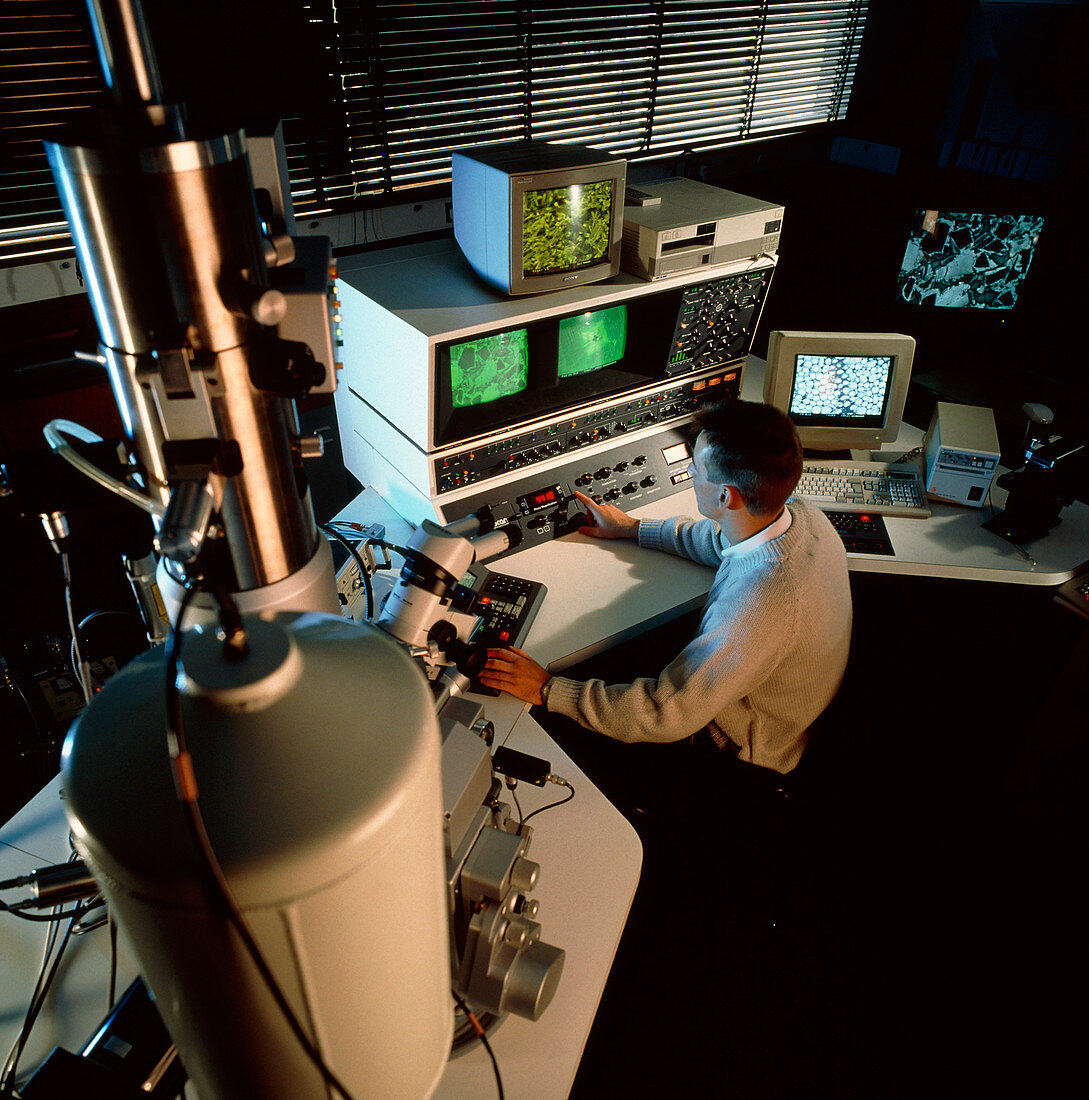
| Scanning electron microscope. Researcher using a scanning electron microscope (SEM,lower left) to study synthetic materials. SEMs use an electron beam to obtain three-dimensional images of objects. The electron beam is swept over the sample,causing secondary electrons to be emitted. These and reflected electrons are used to form the image. Seen on the screens are,from left to right: silicon carbide ceramic,alumina ceramic strengthened with silicon carbide (top),damaged light-emitting sample of magnesium oxide,low- friction surface for textiles,magnified 5000 times,and another silicon carbide ceramic. Photo- graphed at the University of Newcastle,England | |
| Lizenzart: | Lizenzpflichtig |
| Credit: | Science Photo Library / Cuthbert, Colin |
| Bildgröße: | 3506 px × 3543 px |
| Modell-Rechte: | Derzeit liegt noch kein Release vor. Bitte kontaktieren Sie uns vor Verwendung. |
| Eigentums-Rechte: | nicht erforderlich |
| Restrictions: | - |
Preise für dieses Bild ab 15 €
Universitäten & Organisationen
(Informationsmaterial Digital, Informationsmaterial Print, Lehrmaterial Digital etc.)
ab 15 €
Redaktionell
(Bücher, Bücher: Sach- und Fachliteratur, Digitale Medien (redaktionell) etc.)
ab 30 €
Werbung
(Anzeigen, Aussenwerbung, Digitale Medien, Fernsehwerbung, Karten, Werbemittel, Zeitschriften etc.)
ab 55 €
Handelsprodukte
(bedruckte Textilie, Kalender, Postkarte, Grußkarte, Verpackung etc.)
ab 75 €
Pauschalpreise
Rechtepakete für die unbeschränkte Bildnutzung in Print oder Online
ab 495 €