Silicon carbide tip,TEM
Bildnummer 11694802
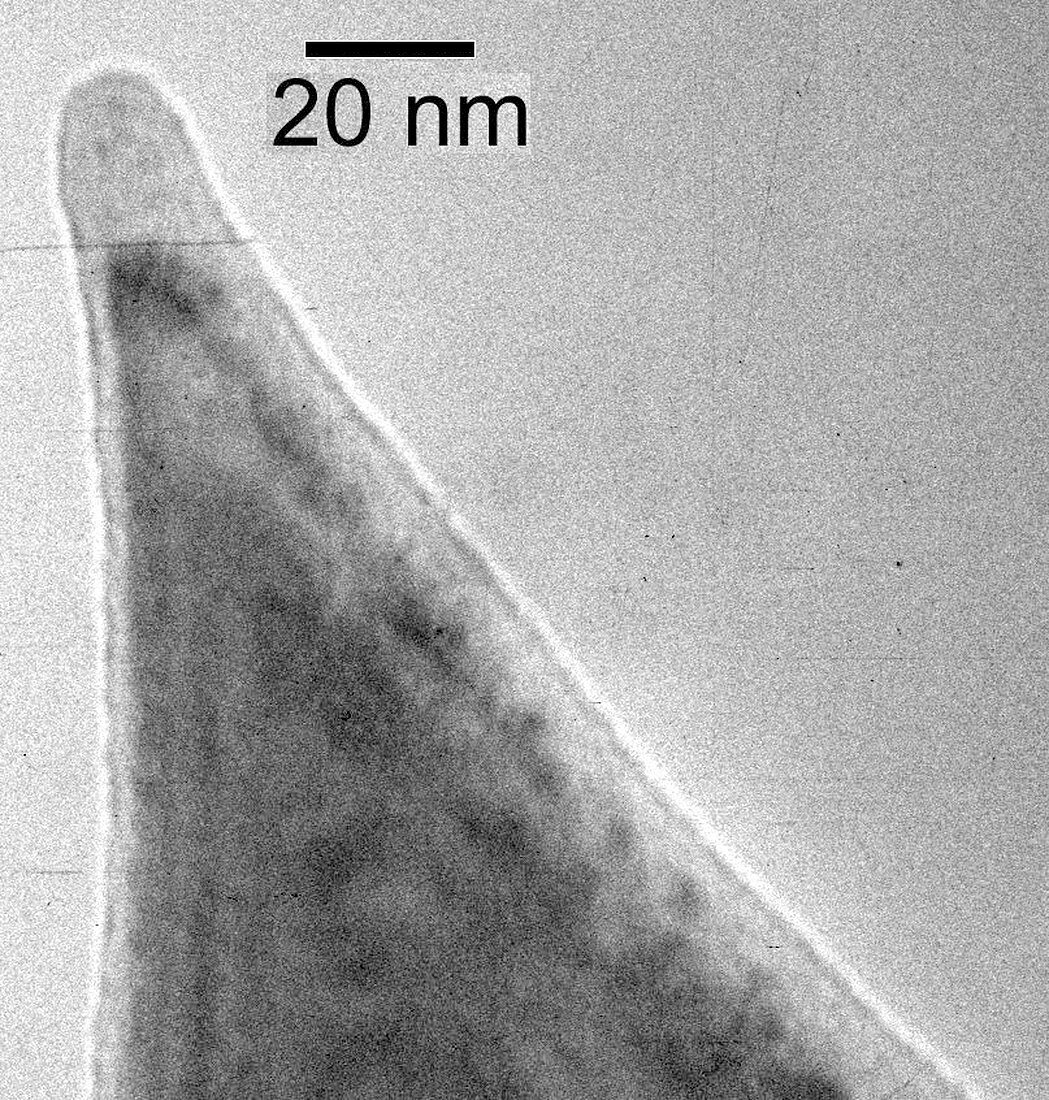
| Silicon carbide tip,transmission electron micrograph (TEM). This ultrasharp silicon carbide tip is thousands of times more wear-resistant at the nanoscale than previous designs. It is 100,000 times smaller than the tip of a pencil and is intended for nanomanufacturing applications such as bio sensors for healthcare and the environment. It was developed by scientists at the University of Pennsylvania,USA,the University of Wisconsin-Madison,USA,and at IBM Research-Zurich,Switzerland. Image published in December 2011. Magnification: x800,000 when printed at 10 centimetres across | |
| Lizenzart: | Lizenzpflichtig |
| Credit: | Science Photo Library / IBM Research |
| Bildgröße: | 3500 px × 3669 px |
| Modell-Rechte: | nicht erforderlich |
| Eigentums-Rechte: | nicht erforderlich |
| Restrictions: | - |
Preise für dieses Bild ab 15 €
Universitäten & Organisationen
(Informationsmaterial Digital, Informationsmaterial Print, Lehrmaterial Digital etc.)
ab 15 €
Redaktionell
(Bücher, Bücher: Sach- und Fachliteratur, Digitale Medien (redaktionell) etc.)
ab 30 €
Werbung
(Anzeigen, Aussenwerbung, Digitale Medien, Fernsehwerbung, Karten, Werbemittel, Zeitschriften etc.)
ab 55 €
Handelsprodukte
(bedruckte Textilie, Kalender, Postkarte, Grußkarte, Verpackung etc.)
ab 75 €
Pauschalpreise
Rechtepakete für die unbeschränkte Bildnutzung in Print oder Online
ab 495 €