Nanowire lithography,IBM research
Bildnummer 11694712
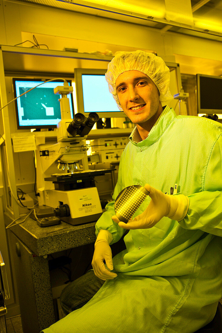
| Nanowire lithography,IBM research. IBM scientist Hesham Ghoneim holding a silicon wafer with lithographically patterned gold pads on top. These are used to contact silicon nanowires. The silicon nanowires are grown via a VLS (Vapor-Liquid-Solid) process and then transferred on to the silicon wafer. Contact leads and gate electrodes are then written with electron beam lithography from the pre-patterned gold pads to the nanowire. Nanowires are a candidate technology for extending current computing capabilities. Photographed in June 2009,at IBM Research-Zurich,Switzerland | |
| Lizenzart: | Lizenzpflichtig |
| Credit: | Science Photo Library / IBM Research |
| Bildgröße: | 2414 px × 3621 px |
| Modell-Rechte: | Derzeit liegt noch kein Release vor. Bitte kontaktieren Sie uns vor Verwendung. |
| Eigentums-Rechte: | nicht erforderlich |
| Restrictions: |
|
Preise für dieses Bild ab 15 €
Universitäten & Organisationen
(Informationsmaterial Digital, Informationsmaterial Print, Lehrmaterial Digital etc.)
ab 15 €
Redaktionell
(Bücher, Bücher: Sach- und Fachliteratur, Digitale Medien (redaktionell) etc.)
ab 30 €
Werbung
(Anzeigen, Aussenwerbung, Digitale Medien, Fernsehwerbung, Karten, Werbemittel, Zeitschriften etc.)
ab 55 €
Handelsprodukte
(bedruckte Textilie, Kalender, Postkarte, Grußkarte, Verpackung etc.)
ab 75 €
Pauschalpreise
Rechtepakete für die unbeschränkte Bildnutzung in Print oder Online
ab 495 €
Keywords
- 21. Jahrhundert,
- eine Person,
- Erwachsene,
- Erzeugung,
- Europa,
- europäisch,
- Forscher,
- gelbes Licht,
- Gold,
- Halten,
- Herstellung,
- kaukasisch,
- Labor,
- Mann,
- Männlich,
- Maschine,
- Mensch,
- Menschen,
- Metall,
- Mikroskop,
- Nanodrähte,
- Nanotechnologie,
- Nanowissenschaftler,
- Person,
- Physik,
- Physiker,
- physisch,
- Reinraum,
- Schweiz,
- schweizerisch,
- Technologie,
- technologisch,
- weiß,
- Wissenschaftler,
- zeigend,
- ZRL,
- Zürich