Semiconductor microscopy,IBM research
Bildnummer 11694580
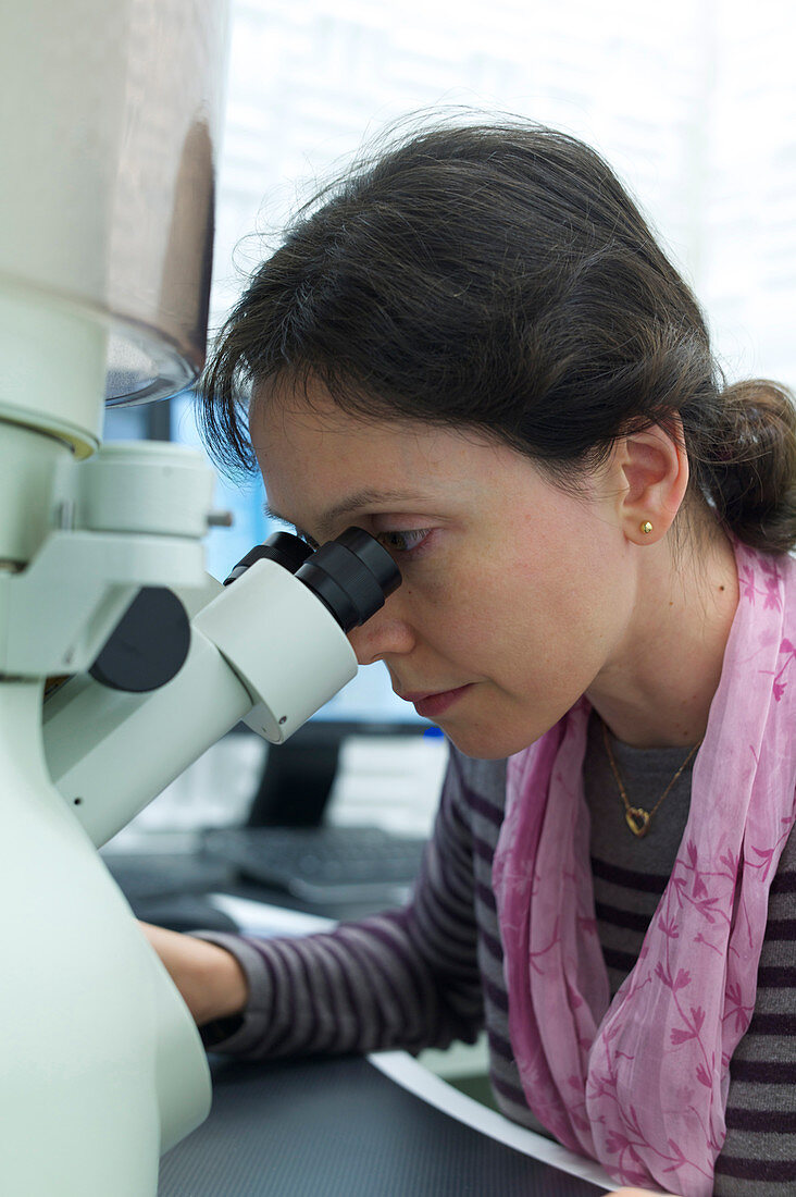
| Semiconductor microscopy,IBM research. French semiconductor engineer Marilyne Sousa using a transmission electron microscope (TEM) in a noise-free laboratory at the Binnig and Rohrer Nanotechnology Center at IBM Research-Zurich,Switzerland. She is part of the Advanced Functional Materials research group,where she performs structural characterization of thin oxide films and III-V materials for high-mobility channels for technology nodes smaller than 14 nanometres. Photographed in October 2013 | |
| Lizenzart: | Lizenzpflichtig |
| Credit: | Science Photo Library / IBM Research |
| Bildgröße: | 2411 px × 3623 px |
| Modell-Rechte: | Derzeit liegt noch kein Release vor. Bitte kontaktieren Sie uns vor Verwendung. |
| Eigentums-Rechte: | nicht erforderlich |
| Restrictions: |
|
Preise für dieses Bild ab 15 €
Universitäten & Organisationen
(Informationsmaterial Digital, Informationsmaterial Print, Lehrmaterial Digital etc.)
ab 15 €
Redaktionell
(Bücher, Bücher: Sach- und Fachliteratur, Digitale Medien (redaktionell) etc.)
ab 30 €
Werbung
(Anzeigen, Aussenwerbung, Digitale Medien, Fernsehwerbung, Karten, Werbemittel, Zeitschriften etc.)
ab 55 €
Handelsprodukte
(bedruckte Textilie, Kalender, Postkarte, Grußkarte, Verpackung etc.)
ab 75 €
Pauschalpreise
Rechtepakete für die unbeschränkte Bildnutzung in Print oder Online
ab 495 €
Keywords
- 2013,
- 21. Jahrhundert,
- Ausrüstung,
- Begutachten,
- Beobachten,
- eine Person,
- Elektronenmikroskopie,
- Erwachsene,
- Europa,
- europäisch,
- forschend,
- Forscher,
- Forschung,
- Französisch,
- Frau,
- Ingenieur,
- kaukasisch,
- Labor,
- Maschine,
- Materialwissenschaft,
- Mensch,
- Menschen,
- Mikroskop,
- Nanotechnologie,
- Oktober,
- Okular,
- Person,
- Physik,
- Physiker,
- Schweiz,
- schweizerisch,
- Technologie,
- tem,
- Transmissionselektronen,
- Weiblich,
- weiß,
- Wissenschaftler,
- ZRL,
- Zürich