Nanotechnology Centre,IBM research
Bildnummer 11694553
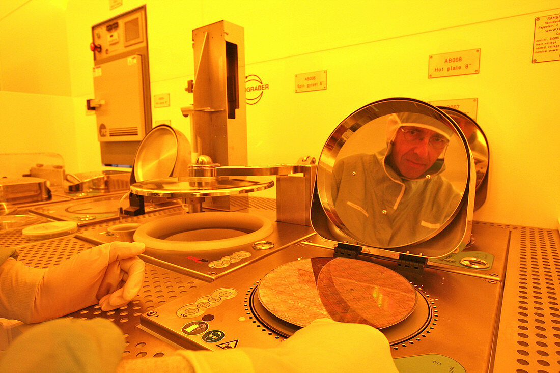
| Nanotechnology Centre,IBM research. German physicist Roland Germann (Manager Nanocenter Operations),with a silicon wafer,in a clean room at the Nanotechnology Centre at IBM Research-Zurich,Switzerland. Processes carried out here in these high-grade clean rooms include lithography,wet processing,wet chemical etching,thin-film deposition,dry etching,thermal processing,and vapour phase deposition. Other processes include plating,lapping/polishing,dicing and bonding,and polymer waveguide processing. Materials include semiconductors (such as silicon),metals,insulators,polymers,organics and oxides. Photographed in 2011 | |
| Lizenzart: | Lizenzpflichtig |
| Credit: | Science Photo Library / IBM Research |
| Bildgröße: | 3620 px × 2413 px |
| Modell-Rechte: | Derzeit liegt noch kein Release vor. Bitte kontaktieren Sie uns vor Verwendung. |
| Eigentums-Rechte: | nicht erforderlich |
| Restrictions: |
|
Preise für dieses Bild ab 15 €
Universitäten & Organisationen
(Informationsmaterial Digital, Informationsmaterial Print, Lehrmaterial Digital etc.)
ab 15 €
Redaktionell
(Bücher, Bücher: Sach- und Fachliteratur, Digitale Medien (redaktionell) etc.)
ab 30 €
Werbung
(Anzeigen, Aussenwerbung, Digitale Medien, Fernsehwerbung, Karten, Werbemittel, Zeitschriften etc.)
ab 55 €
Handelsprodukte
(bedruckte Textilie, Kalender, Postkarte, Grußkarte, Verpackung etc.)
ab 75 €
Pauschalpreise
Rechtepakete für die unbeschränkte Bildnutzung in Print oder Online
ab 495 €
Keywords
- 2011,
- 21. Jahrhundert,
- Ausrüstung,
- Betrachtung,
- Center,
- Computerwesen,
- Deutsche,
- eine Person,
- Erwachsene,
- Europa,
- europäisch,
- forschend,
- Forscher,
- Forschung,
- gelbes Licht,
- ISO 7,
- kaukasisch,
- Klasse 100,
- Klasse 10000,
- Labor,
- Manager,
- Mann,
- Männlich,
- Materialwissenschaft,
- Mensch,
- Menschen,
- Nanotechnologie,
- nasschemisches Ätzen,
- Nassverarbeitung,
- Person,
- Physik,
- Physiker,
- physisch,
- Reinraum,
- Schweiz,
- schweizerisch,
- Studium,
- Technologie,
- technologisch,
- weiß,
- Wissenschaftler,
- ZRL,
- Zürich