Nanowires on nickel, SEM
Bildnummer 12258293
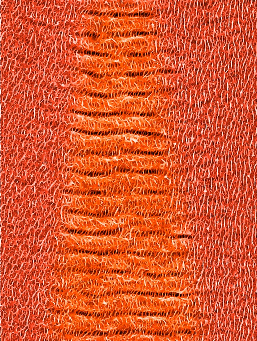
| Nanowires on nickel. Coloured scanning electron micrograph (SEM) of nanowire structures formed on a nickel surface by pulses of a laser beam. This research involves the use of lasers to etch and ablate metal and semiconductor surfaces. The resulting nanostructures can have applications in various forms of electronics and nanotechnology. | |
| Lizenzart: | Lizenzfrei |
| Credit: | Science Photo Library / GEORGY SHAFEEV |
| Modell-Rechte: | nicht erforderlich |
| Eigentums-Rechte: | nicht erforderlich |
| Restrictions: | - |
Preise für dieses Bild ab 29 €
Für digitale Nutzung (72 dpi)
ab 29 €
Für Druckauflösung (300 dpi)
ab 300 €